Nano Positioning Devices
Ratis – nano piezo stage for nanopositioning and scanning
Ratis is a family of plane-parallel piezo stages for nanopositioning and scanning developed by NST. Ratis piezo stages are capable of moving the objects with sub-nanometer precision. Their unique feature is a large aperture (45 mm in diameter) in the center while outer dimensions are only 100х100 mm. This could be useful in applications require clear optical path in the center of the stage.
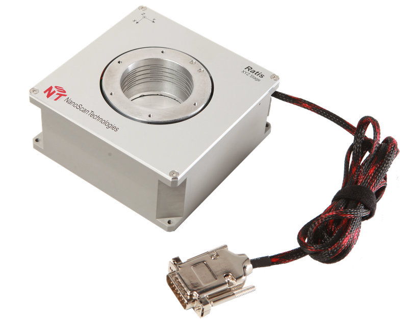
Piezo stages are made of solid metal bar processed with EDM wire-cutting and precise CNC machining. Movable central part hangs on flexible springs and is driven with piezo actuators. Ratis design provides excellent linearity and flatness of the movement, in contrast to the classical scanners based on piezoelectric tubes, where the scan surface is a sphere. In addition, plane-parallel scanners have higher mechanical strength, compared with fragile piezoelectric tubes.
Ratis multi-axes scanners are equipped with capacitive displacement sensors for digital closed-loop control. It provides high accuracy and linearity of movement and eliminates the creep effect of piezoceramics. Capacitance measurements are made with TDC (time-to-digital conversion) technology where all measuring electronics is located as close as possible to the sensors. Such a design leads to the low noise and high speed displacement control.
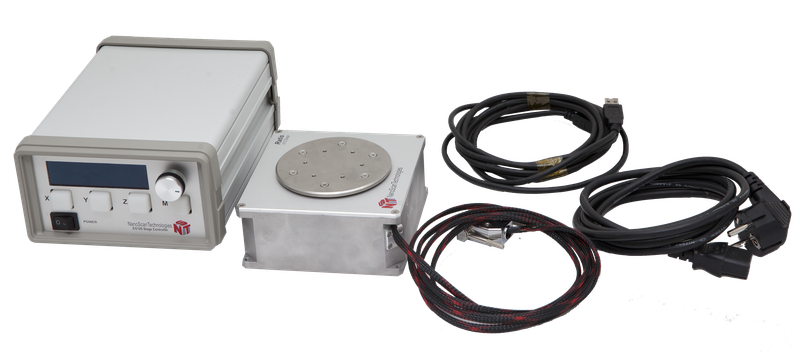
To control Ratis piezo stages universal controllers EG-5000 or EG-1100 are used as well as NSpec software.
Applications of Ratis include scanning probe microscopy (e.g. atomic force microscopy), nanopositioning, metrology, biology research, microelectronics, micromanipulation etc.
Optical sensors
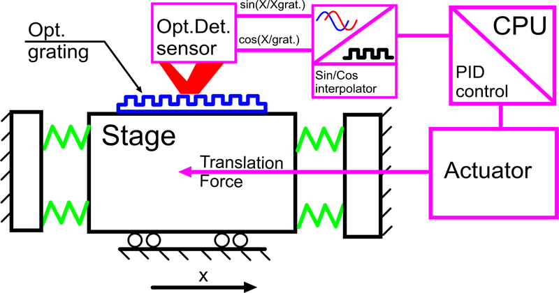
The scanning stage Ratis uses optical sensors. The principle of operation of such sensors is shown in Figures. The displacement sensor consists of an
optical ruler, a period of 10 μm or 20 μm, a radiation source of a red light diode, and a selective radiation detector outputting signals shifted in phase by 90 degrees:
A(x)=A0×sin(X/Xgrat)
В(x)=B0×cos(X/Xgrat)
X – translation,
Xgrat – optical grating period.
 |
 |
These signals in analog form are processed by a specialized microchip with built-in sin/cos interpolator, producing the angle calculation as arctg (A/B). Thus, the movement is reduced to calculating the angle, then the chip converts the angle into pulses, which are formed when the minimum detectable angle α of rotation is exceeded.
Then the movement is calculated as:
X =Sn× α× Хgrat, Sn- Sum of pulses from a specialized counter.
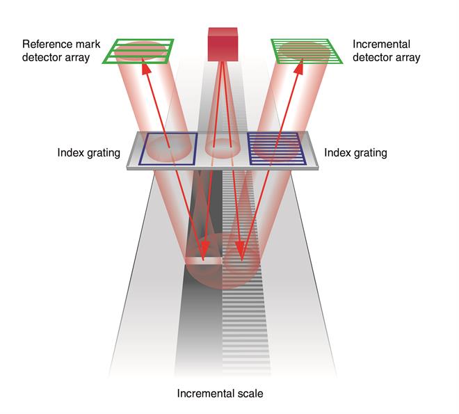
Optical sensors produce displacement calculations along a special plate, on which lines are plotted with a specified period. Lines are caused by interference of waves with given lengths, which leads to high accuracy of the length of the period of these divisions. When measuring a distance, the number of periods or the part of the period that the sensor has passed is calculated. Since all the phenomena in this sensor are correlated to the wavelengths, the accuracy of the measurements is quite high.
Full article: Optical Sensors
Double Cap Technique
Capacitance sensors are mostly used as translation sensors, in various positioning systems. It is quite simple and cheap. Typical system is drawn in pic 1. One capacitance (C1, or C2) is normally used for displacement measurement, signal are being processed with PID controller, and calculated force are being applied to control object. Quite big disadvantage is nonlinear response from sensors(pic 2. C1(x) dependence, or C2(x)), it can be written as C(x) ~, this dependence causes 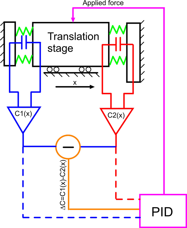 different sensors response at the beginning and end of the translation range, up to 10 times which leads to problem with PID controller tuning, and different resolution (accuracy), it means quite big translater non-uniformity. Nano Scan Technologies uses advanced technology based on two sensors measurement, which arranged at opposite sides of the scanner. When first capacitance is increasing, another is decreasing. This can be written as following dependence: D C ~ - ; You can see this dependence at Pic. 2. Linearity of this curve is much better for system linearization, response difference is much smaller, just 2 times, scanner becomes more uniform in resolution and linearity terms. This technology is using in all our scanners, Ratis model.
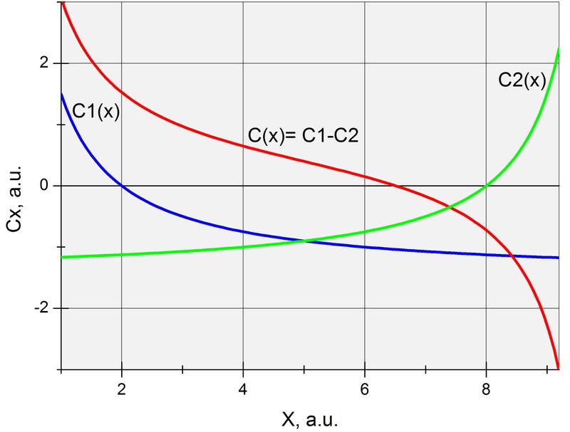
| Parameters | Ratis XY(Z)_H | Vectus Z stage |
Ratis 1X |
| XY travel range, µm | 100×100 | ---------- | ------------- |
| Z range (Closed-Loop), µm | 50 | 60, 100 | 120 |
| Resonant frequency XY, kHz | 1 | ---- |
-------- |
| Resonant frequency Z, kHz | 3 | 3 | 3 |
| Minimum scan step, nm | 0.1 | 0.1 | 0.1 |
| Angle tilting over the full range, nm | < 0.01° | < 0.01° | < 0.01° |
| Maximum scanning speed, Hz (line/sec) | 10 | 10 | 10 |
| Base sample weight, g | 100 | 100 | 100 |
| Operating temperature range | at -40°C to 80°C | at -40°C to 80°C | at -40°C to 80°C |
| Dimensions, mm | 100×100×30 | 100×100×35 | 100×100×35 |
| Clear aperture diameter, mm | 45 | ---- | ------- |
| Material | Aluminium | Aluminium | Aluminium |
| *Optional range |
* | * |